Customer Test: 300W Pulsed Laser Cleaning for Semiconductor Reflow Carrier Trays
Semiconductor reflow carrier trays, also called oven carrier trays or high-temperature process trays, are used to hold chips, lead frames, substrates and electronic components as they pass through baking, reflow soldering, sintering, curing and aging processes. For semiconductor packaging, SMT assembly, power devices, discrete devices and IC packaging lines, these trays are not simple containers. They are precision process tooling that must keep parts stable while resisting heat, deformation and contamination.
Customer On-Site Sample Test
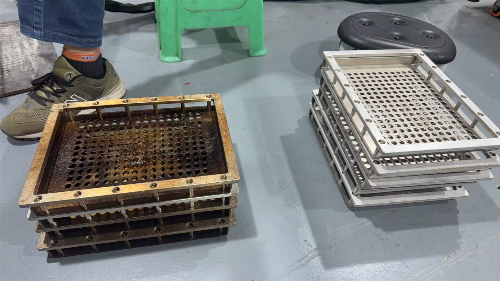
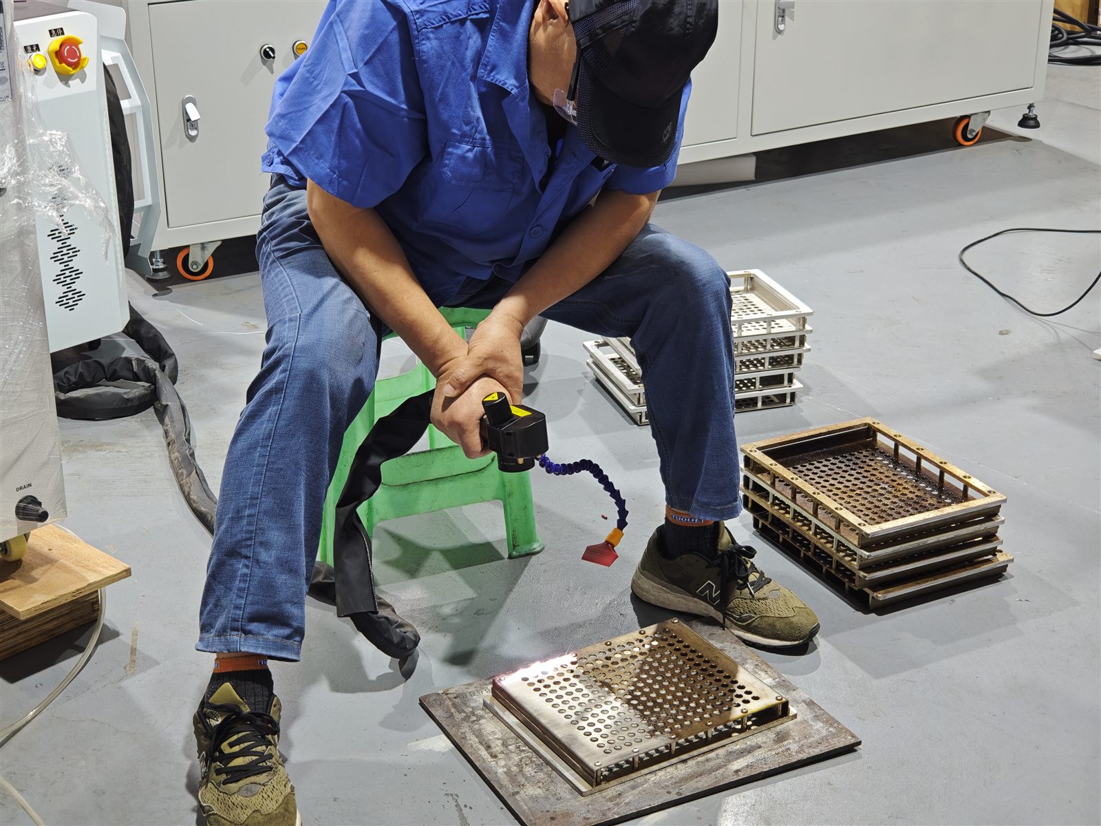
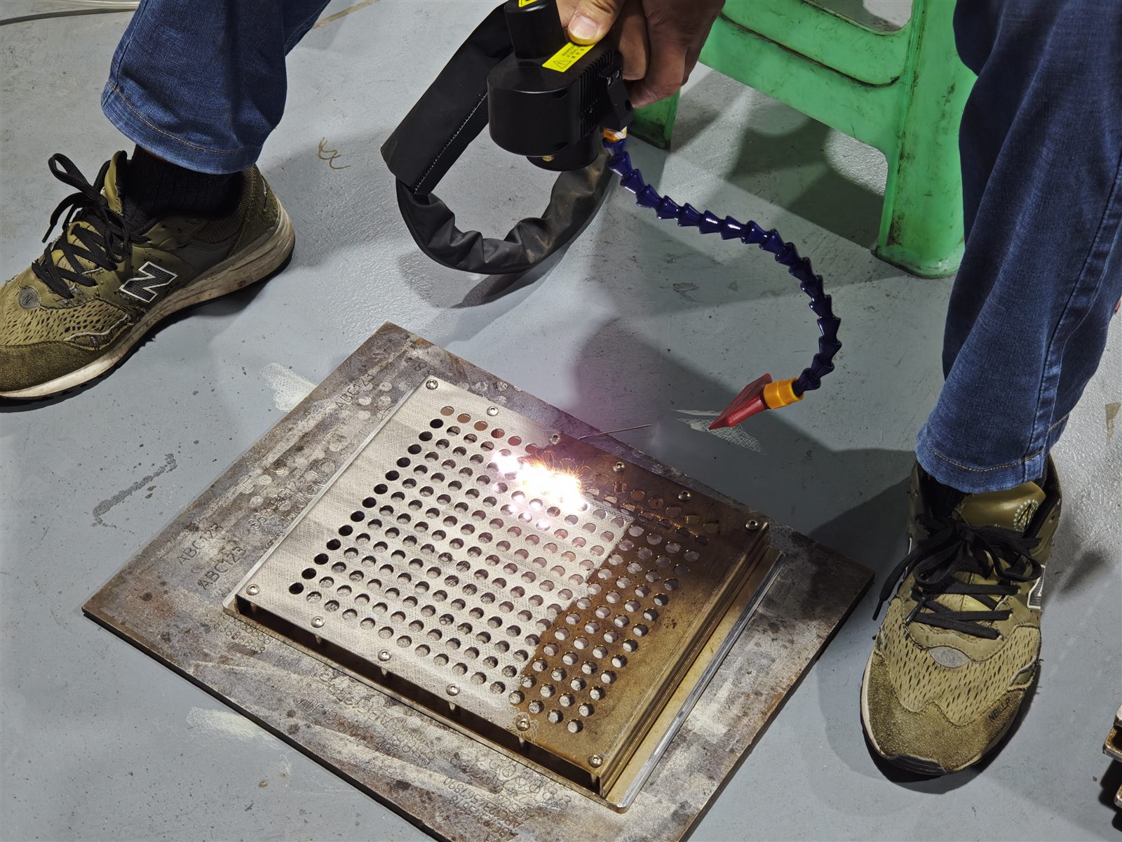
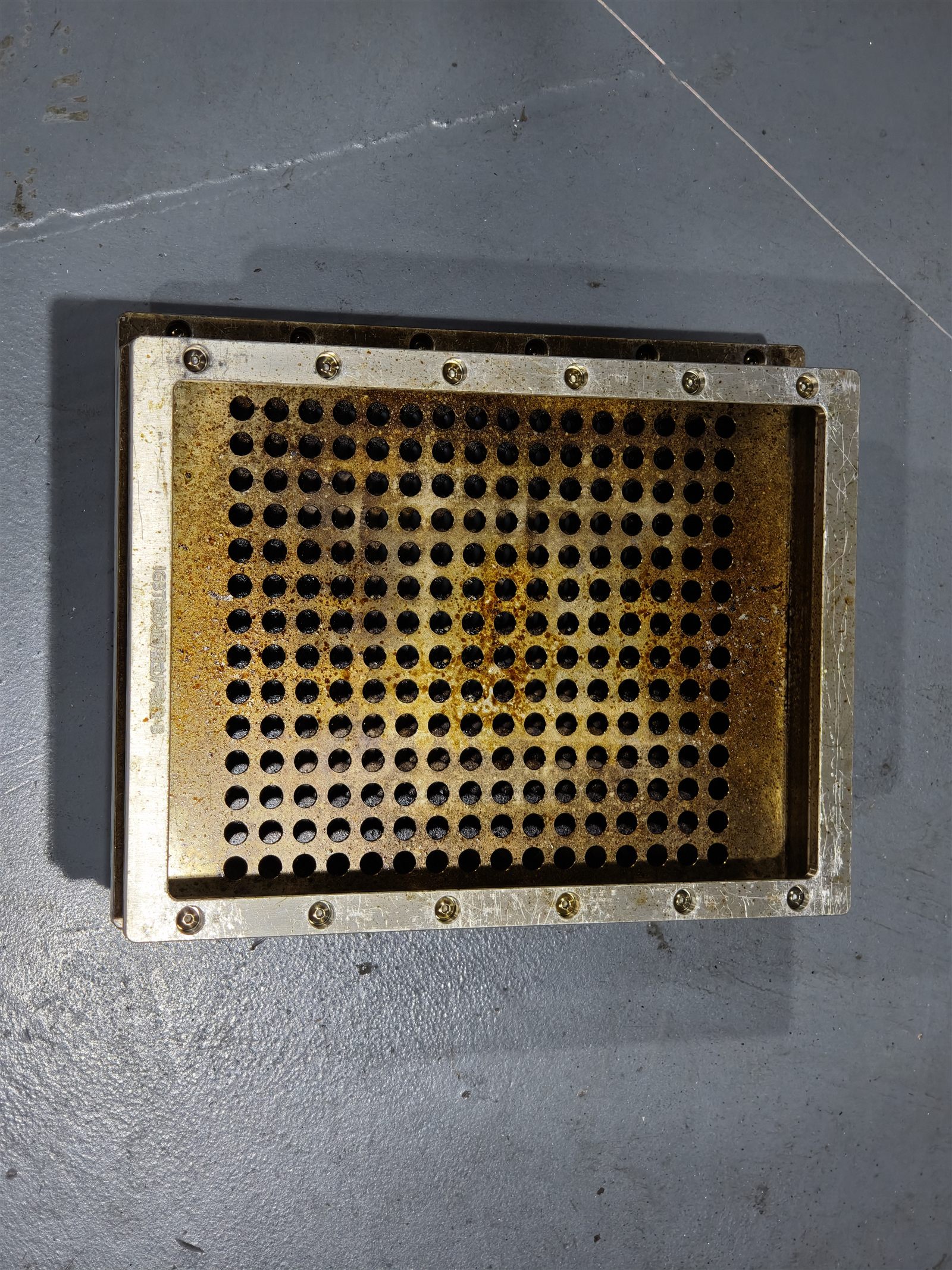
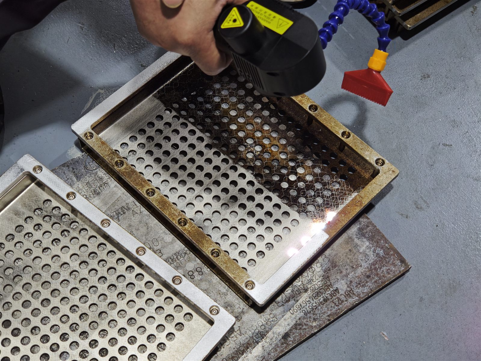
A customer visited Chongqing Zixu Machine Works for a sample cleaning test and operated the 300W pulsed laser cleaning equipment by themselves. The test focused on used semiconductor carrier trays with visible process residue. The purpose was to evaluate whether pulsed laser cleaning could remove surface contamination from high-temperature trays while reducing the dependence on manual scraping, chemical soaking or abrasive treatment.
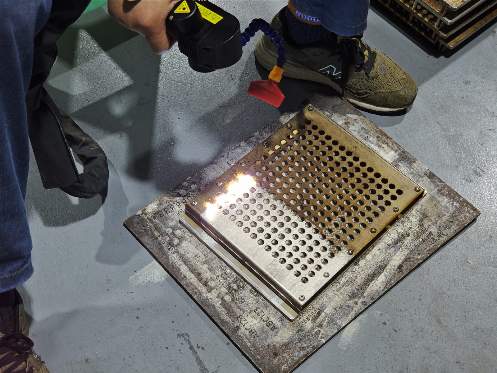
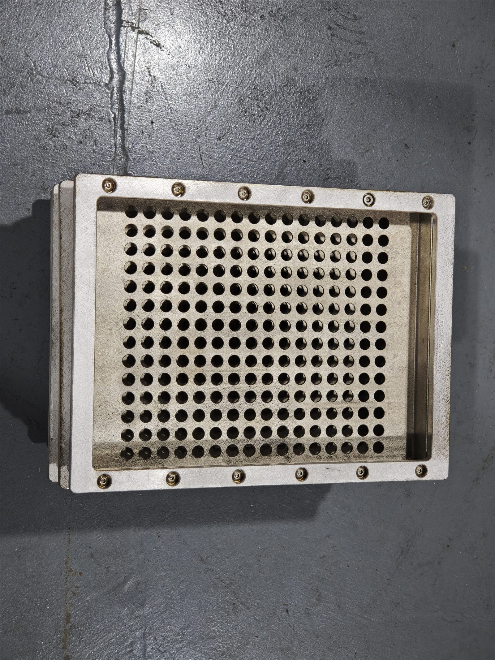
During the test, the 300W pulsed laser cleaning system was applied directly to the tray surface. The non-contact laser beam removed residue from the working area of the tray, giving the customer a practical view of cleaning speed, surface response and operating feel. The photos show the real sample-testing process rather than a staged production line installation.
Where Reflow Carrier Trays Are Used
These carrier trays are widely used in high-temperature semiconductor and electronics manufacturing steps. In pre-packaging baking and dehumidification, bare dies, frames and components are placed on trays and moved into ovens to remove moisture before encapsulation, helping reduce blistering and delamination risk. After molding, trays support lead frames or substrates through molding cure and post-molding cure processes.
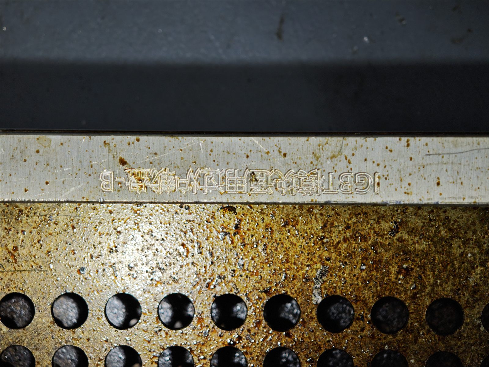
In SMT reflow soldering and ball attach reflow, BGA, QFN and power devices may require heat-resistant trays to keep the part position stable while solder balls or solder joints are formed. In power semiconductor manufacturing, IGBT modules, MOSFET devices, SiC power modules and DBC ceramic substrates may use carrier tooling during high-temperature sintering, silver sintering, baking and thermal cycling.
For wafer-level packaging, MEMS and micro-assembly, trays may be used during annealing, metallization annealing and reliability testing. The cleaning needs vary by tray material. Graphite, ceramic, quartz, high-temperature PEEK and hard-anodized aluminum alloy each respond differently to laser parameters.
Why Pulsed Laser Cleaning
After repeated high-temperature use, carrier trays collect flux residue, oxide layers, carbonized organic residue, solder splash, adhesive residue, oil, dust and discoloration. These contaminants may affect component placement accuracy, heat transfer consistency, product appearance and long-term process stability.
Pulsed laser cleaning is a dry, non-contact method. It removes contamination without chemical soaking, abrasive grinding or manual scraping. For semiconductor fixtures and high-temperature tooling, this means less consumable usage and less secondary waste compared with traditional methods.
Customer Test Outcome
The customer operated the 300W pulsed laser cleaning machine by themselves and saw real-time cleaning results on their used trays. The test showed that pulsed laser cleaning can remove residue from reflow carrier tray surfaces without chemical treatment. This is useful for semiconductor packaging lines, SMT reflow lines, power device manufacturing and electronics assembly where tray maintenance is an ongoing task.
Each factory has different tray materials, residue types, process temperatures and cleanliness requirements. A sample test with real parts is the most practical way to evaluate whether laser cleaning fits a specific production workflow.
About CNMarking
CNMarking Chongqing Zixu Machine Works offers pulsed laser cleaning machines for semiconductor manufacturing support, SMT production and electronics assembly tooling maintenance. Customers are welcome to bring their own trays and parts for on-site sample testing.